
1. Context and Motivation
High-resolution delta-sigma ADCs promise impressive performance on paper, but realizing that performance in real hardware requires careful attention to architectural constraints that are easy to overlook.
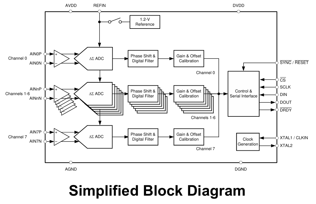
This post documents practical observations from implementing the ADS131M08, a multi-channel 24-bit delta-sigma ADC, in an embedded system. The focus is not on basic usage, but on less obvious behaviors that materially influence front-end design, clocking, filtering, and system reliability. The ADS131M08 can deliver excellent performance, but its input range, digital filtering, clocking, and DRDY behavior impose non-obvious constraints that matter in real embedded systems.
2. Why the ADS131M08 Is Attractive
At a high level, the ADS131M08 offers a compelling combination of features:
-
24-bit resolution with integrated digital filtering
-
Multi-channel simultaneous sampling, well suited for sensor and force arrays
-
Configurable bandwidth via oversampling ratio (OSR) control
-
Wide temperature rating for industrial and embedded environments
-
Compact package and favorable cost-to-performance ratio
For applications requiring low-frequency, high-resolution measurements across multiple channels, this class of ADC is difficult to replace.
These advantages, however, come with architectural constraints that differ significantly from more familiar SAR-based converters.
3. Delta-Sigma Architecture: Input Range Is Not What You Expect
One of the first practical challenges is understanding the allowed input voltage range, which is not simply bounded by ground, supply, or reference in the way many designers expect.
Absolute Input Voltage Limits
When operating with gains of 1, 2, or 4, the allowed absolute input range is:
-
AGND − 1.3 V to AVDD
When the programmable gain amplifier is set to 8 or greater, the range tightens to:
-
AGND − 1.3 V to AVDD − 1.8 V
This behavior is atypical for precision ADCs and has direct implications for front-end biasing, protection, and fault tolerance. Notably, even when supplying signals nominally between GND and AVDD, the input structure expects tolerance for voltages extending below ground.
Differential Input Range
When using the internal reference, the differential input voltage is constrained to:
-
±(Vref / Gain)
As gain increases, usable signal swing compresses rapidly—even when absolute input limits are respected.
External Reference Constraints
The external reference input introduces an additional limitation:
-
Vref(ext) must lie between 1.1 V and 1.3 V
This narrow window further constrains system-level design and eliminates some otherwise convenient reference strategies.
Taken together, these constraints are easy to miss and can result in designs that appear valid on paper but clip or fail in practice.
4. Clocking Requirements and Oversampling Tradeoffs
Unlike many ADCs that accept flexible clocking schemes, the ADS131M08 requires an external clock, with an allowable range of approximately:
-
0.3 MHz to 8.4 MHz
This clock directly interacts with the oversampling ratio (OSR), affecting output data rate, noise performance, and group delay. Because the internal digital filtering is tightly coupled to this clock, clock stability and jitter become more significant than they might appear in lower-resolution systems.
5. Fast-Settling and SINC Filter Behavior: Practical Limitations
The ADS131M08 includes internal SINC and fast-settling digital filters that provide convenient decimation and noise shaping. While effective for suppressing out-of-band noise, these filters are not always well suited for systems in which passband fidelity matters.
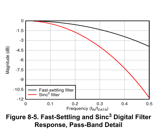
A key limitation is that the SINC filter does not provide a flat passband. As shown in the datasheet frequency-response plot (Figure 8-5), attenuation begins immediately as frequency increases from DC. Even well below the nominal cutoff, measurable roll-off is present, which can distort amplitude information within the intended measurement band.
This behavior is inherent to SINC-based decimation filters and is often acceptable for quasi-static measurements. However, in dynamic or mechanically coupled sensor systems—where bandwidth, phase, or amplitude accuracy matters—this early roll-off can become a limiting factor.
When system resources allow, it is often preferable to minimize reliance on the internal SINC filter, operate the ADC at a higher output data rate, and implement additional filtering downstream in the microcontroller. A tailored FIR or IIR filter allows:
-
Explicit control over passband flatness
-
Predictable amplitude and phase response
-
Better alignment with application-specific frequency requirements
The internal filters remain useful as a first stage of noise shaping, but are best treated as a convenience rather than a complete signal-conditioning solution.
6. Data Ready (DRDY) Signaling: Datasheet Semantics vs. Firmware Reality
The DRDY signal warrants special attention, as it can be a source of subtle and frustrating bugs if interpreted too literally.
According to the datasheet (MODE register, DRDY_FMT bit), two DRDY formats are supported:
-
DRDY_FMT = 0: DRDY transitions high-to-low and remains low until
-
all conversion data are shifted out, or
-
DRDY briefly transitions high before the next conversion cycle
-
-
DRDY_FMT = 1: DRDY produces a short negative pulse; if data are not read after this transition, subsequent behavior can be ambiguous
While documented, the practical implications are easy to underestimate.
In practice, certain configurations cause DRDY to pulse high briefly before the conversion is fully complete, even though the next data frame is not yet valid. If firmware triggers an interrupt on this transition without qualification, the result can be:
-
Interrupts firing before data are ready
-
Partial or invalid reads
-
Apparent “double-pulse” behavior
When DRDY was used directly as an interrupt source, the initial transition triggered the ISR prematurely—well before conversion data were stable.
The workaround was to treat the first DRDY transition as provisional, ignore it explicitly, and act only on a qualified second event. This required firmware state tracking, timing-based qualification, and validation checks before data processing.
The key lesson is that DRDY is not a simple “conversion complete” signal. Robust firmware must explicitly account for DRDY format configuration and tolerate intermediate transitions that do not correspond to usable data.
7. Known-good configuration (baseline that worked reliably)
Interface / Framing
-
SPI framing: 16-bit word mode (MODE = 0x0004)
-
DRDY interrupt enabled after register configuration and readback verification
PGA Gain
-
GAIN1 and GAIN2 set identically, selected from nonvolatile configuration
-
Gain codes:
x1 (0x0000), x2 (0x1111), x4 (0x2222), x8 (0x3333),
x16 (0x4444), x32 (0x5555), x64 (0x6666), x128 (0x7777)
Gain is applied uniformly across channels using replicated nibble patterns.
Data Rate / Filtering
-
OSR = 512 via CLOCK/OSR register write (0xFF0B, 4-channel variant)
Initialization Sequence
-
Set MODE → delay
-
Set GAIN1 → delay
-
Set GAIN2 → delay
-
Set OSR → delay
-
Read back registers
-
Enable DRDY interrupt
8. Implementation notes that mattered in practice
1) “16-bit mode” was a robustness choice
Using 16-bit output words simplified SPI framing and reduced alignment and synchronization errors during bring-up. This was particularly helpful while debugging DRDY timing.
In practice, noise performance improved by increasing analog gain rather than relying on full 24-bit digital resolution. The additional digital bits did not translate into usable signal quality once system-level noise was considered, whereas higher front-end gain improved effective in-band resolution.
This reinforced the importance of treating nominal ADC resolution and effective system resolution as separate concerns.
2) DRDY_FMT behavior can break naïve ISR logic
Certain DRDY formats introduce intermediate transitions that can trigger interrupts prematurely. Without explicit qualification logic, this led to ISR execution before valid data were available, producing nondeterministic behavior despite correct ADC operation.
3) Guard delays between register writes mattered
Introducing short delays between MODE → GAIN → OSR writes, and before enabling DRDY interrupts, eliminated intermittent startup failures. Although back-to-back writes should be tolerated, these guard delays made initialization behavior deterministic.
4) MODE = 0x0005 caused acquisition to freeze in this build
In this configuration, DRDY was used to trigger data reads. If a DRDY event was missed, subsequent conversions halted, freezing acquisition. This behavior made MODE = 0x0005 unsuitable for interrupt-driven operation and it was avoided.
9. Closing Observations
The ADS131M08 is a capable device, but it rewards careful attention to both datasheet details and real-world behavior.
Key takeaways:
-
Input voltage limits are more constrained—and less intuitive—than many ADCs
-
Reference selection and gain are tightly coupled
-
Clocking strategy directly impacts performance and usability
-
Digital filtering and DRDY behavior require deliberate firmware design
For designers accustomed to other ADC architectures, these differences matter—and misunderstanding them can easily lead to multiple rounds of rework.
Related notes: Practical FIR filtering choices for embedded sensor systems.